Paper
Solving AI Semiconductor Power Shortages
with a Glass-Based Optical Platform
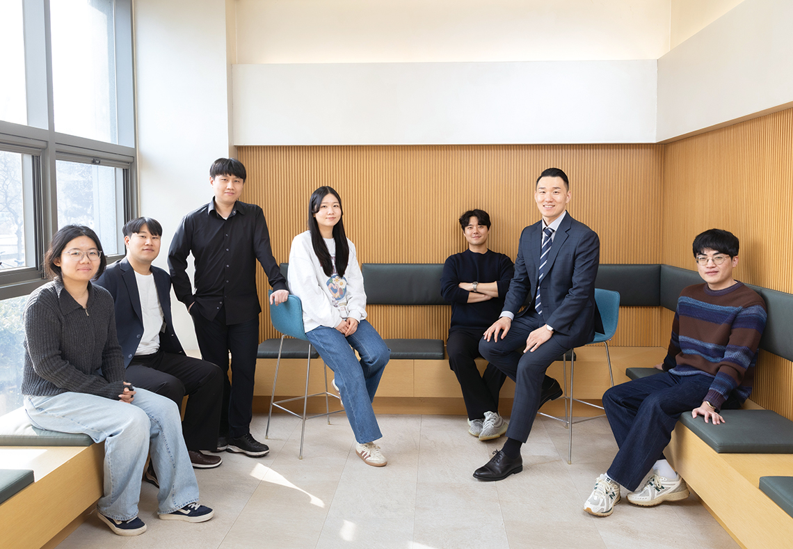
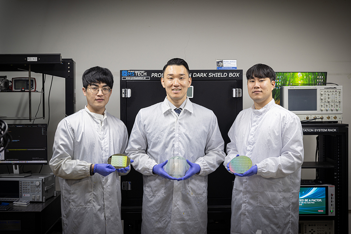
ASDL AI Semiconductor Driving Laboratory
Professor YoungHyun Kim and researchers TaeWonJin and HeeYun Jung
- Written by. YeongIm Park
- Photo by. ChoWon Son


Ultimately, it’s the Energy!
Last January, the U.S. Trump Administration urgently proposed a bid for the construction of power plants to address the power shortage triggered by the rapid growth of AI data centers. The underlying intention was to pass on the electricity costs to big tech companies. Several big tech companies have already been building their own power-generation facilities, and Tesla CEO Elon Musk recently captured the spotlight by announcing plans to build a space-based data center powered by solar energy and radiating heat. All of these events result from the fact that AI consumes enormous amounts of electricity to perform reasoning and computation.
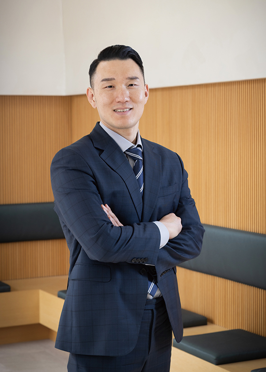
“The problem lies with energy. While the rapid advancement of AI technology has made our lives more convenient, it comes with massive social costs resulting from explosive energy consumption. It is difficult to resolve this energy crisis with the current used wired communication that involves copper interconnections. By making use of light however, the core issues of energy consumption and heat generation in AI semiconductor chips can be solved, according to Professor YoungHyun Kim.
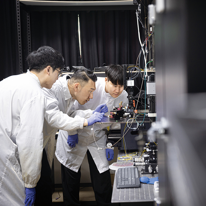
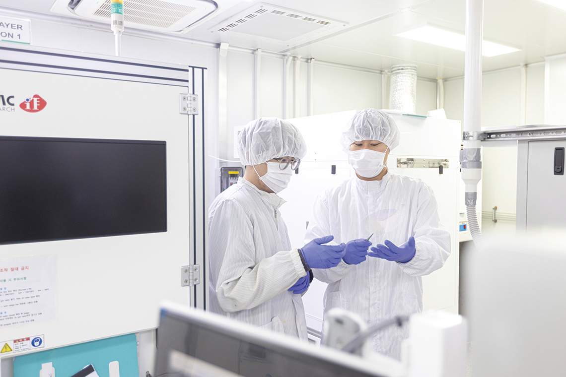
This is why Professor Kim, who leads the AI Semiconductor Driving Laboratory (ASDL), is dedicated to developing optical communication technology that reduces energy consumption by increasing data transmission efficiency. ASDL has already secured proprietary technology of advanced photonics packaging technology which is capable of designing, fabricating, evaluating, and analyzing photonic devices on glass substrates. The result is the overcoming of the limitations of conventional copper interconnections. In November 2025, ASDL unveiled a next-generation “glass-substrate-based silicon nitride (SiN) photonic integrated platform”.
This research was recognized for its excellence by demonstrating for the first time in the world the ”silicon nitride photonics on glass (SING) platform,” a next-generation photonic redistribution layer based on a glass substrate at the wafer level. By utilizing silicon nitride and metal reflectors, the lab proved an integration density more than 10-times higher than existing technologies and an ultra-high-speed transmission performance of 106 Gbps. This research is significant in that it has opened up the possibility of localizing photonic foundry technology, since Korea has been previously dependent on supplies from overseas. In fact, ASDL successfully transferred technology worth KRW500 million to a related company.
Participating Researchers also Published Papers in International Academic Journals
An even more meaningful achievement of the project is that the participating researchers developed their respective areas of expertise and successfully published the research results in international academic journals. For example, research titled, “Glass-based Silicon Nitride Photonics Platform for Scalable High-Density Photonic Redistribution Layers in Panel-Level Packaging,” led by researcher TaeWon Jin (25 years old, Ph.D. student in the Department of Photonics and Nanoelectronics) was published in “Optics Express,” an SCI-indexed journal in the fields of advertising and photonics.
“It is said that AI model performance doubles every six months. To sustain this trend, new technologies capable of addressing bandwidth and power consumption issues are essential. We have proven that a glass-based silicon nitride platform is suitable for an integrated photonics platform to handle the increasing volume of AI computation.”
In addition, Researcher HeeYun Jeong (25 years old, student of the Integrated Master's and Doctoral Program in the Department of Photonics and Nanoelectronics) conducted research on “Implementation of SiNGrating Coupler with Metal Reflector on Glass Substrate” and was able to have the results published in “IEEE Photonics Technology Letters.” Prior to this, Jeong also published the final design results that formed the basis of the aforementioned research in the Japanese Journal of Applied Physics (JJAP).
“If the paper presented in JJAP demonstrated the feasibility of the design, the second paper proved overwhelming performance through actual processes and measurements, verifying the figures I designed with experimental data. I felt a great sense of accomplishment as an engineer,” Jeong said.
Advancing Toward an Era of Sustainable AI
Professor Kim usually actively encourages researchers to present papers at international conferences or in academic journals. He even personally checks the deadlines to ensure that the researchers do not fall behind.
“I believe nurturing outstanding engineers is one of my important callings. It is my greatest reward to watch researchers grow into experts with deeper knowledge than me. I always urge my researchers to conduct research that contributes to the industry,” Kim said.
He founded the company, YK Photonics, last August, setting a good example for other researchers. Professor Kim decided to start the company with the sole intention of contributing to society, as he had been struggling with his own research due to the lack of commercialized photonics foundry infrastructure in Korea. The goal of YK Photonics is to develop eco-friendly and efficient optical communication technology for the industry. To this end, the company pledges to move forward steadfastly and diligently.
MINI INTERVIEW
 Researcher TaeWon Jin(25 years old, Ph.D. student in the Department of Photonics and Nanoelectronics)
What do you think are the important qualities needed for a young researcher?
Researcher TaeWon JinI believe curiosity is the most important. To consistently pursue a career in research, one must have the habit of questioning and investigating why things happen the way they do, whether it is devices observed during research, the research methods of senior colleagues, or the usage of equipment manuals during experiments. The second quality necessary is persuasiveness. Even the most groundbreaking discovery is useless if one cannot persuade others of its value. Therefore, I would actually say this quality is more important than the first.
What are your future research plans and goals?
Researcher TaeWon JinMy first goal is to conduct research into various photonic devices within integrated optics and conduct applied research applicable to actual industries. Based on these efforts, my second goal is to develop a new concept of a device that works with ferroelectrics, which was the topic of my master’s thesis. I want to become a researcher and an engineer who can contribute to real industries, leveraging the expertise I have accumulated in the field of integrated optics.
 Researcher HeeYun Jeong(25 years old, student in the Integrated Master's and Doctoral Program in the Department of Photonics and Nanoelectronics,)
Please briefly explain your research titled, “Implementation of SiNGrating Coupler with Metal Reflector on Glass Substrate” published in an international academic journal”.
Researcher HeeYun JeongGlass substrates, which are in the spotlight as next-generation semiconductor substrates, have a fatal drawback: light tends to leak downwards resulting in reduced optical coupling efficiency. To solve this problem, I developed a silicon nitride-based grating coupler used on a glass substrate containing a metal reflector. This way, I could prevent light loss and improve optical coupling loss by more than 4.3 dB compared to existing methods. I also demonstrated the feasibility of actual commercialization through ultra-high-speed data transmission tests.
What are your future research plans and goals?
Researcher HeeYun JeongMy short-term goal is to fabricate world-class photonic devices at the Sub-dB level (less than 1dB), which is the theoretical limit, by drastically reducing optical coupling losses. And in the long term, I hope my lab’s technology becomes a global standard, serving as a foundation for Korea to lead the CPO and next-generation glass substrate packaging markets. Also, I want to develop into a researcher who can change paradigms in the actual industrial field, going beyond theory.