ERICA's Brain
Technology that will greatly increase market competitiveness of short-wave infrared cameras developed for the first time in the world
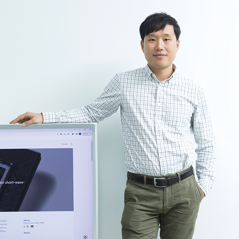
Ji-won Lee, Professor of the Dept. of Photonics and Nanoelectronics
The “pinned photodiode-based image sensors” developed by Professor Ji-won Lee of the Department of Photonics and Nanoelectronics at ERICA is a technology that is drawing keen attention as it can effectively lower processing costs while maintaining high image-quality of short-wave infrared (SWIR) cameras. Any technology that can help to overcome problems of existing technologies while maintaining high performance is expected to have a great impact in both the market and the industry.
- Written by · Yeon-joo Lee
- Photo by · Hyeon-gu Lee


Pinned photodiode-based image sensors?
Short-wave infrared (SWIR) cameras can secure sights even in bad weather or environments that have smoke or thick fog, and even in the darkness of night. This technology has a very high industrial value as it can be applied to capture scenes of delicate objects, or be used to observe stars in the night sky. It can even be used to unlock a smartphone using the facial recognition feature at the bottom of the display. In order to maintain high image quality, SWIR cameras use group III-V compound based semiconductors (InGaAs), which was introduced as a core material for short-wave infrared usage because it has higher electron mobility and lower power consumption than silicon semiconductors. However, the high manufacturing process cost of group III-V semiconductor materials had been a major disadvantage. This is why SWIR cameras cost tens of millions of Korean won. Thus, it was used only in specific fields such as national defense and space development.
To overcome the problems of material and processing costs, technology was introduced to detect shortwave infrared rays by integrating quantum dots on silicon wafers. However, this also caused problems in the form of poor noise performance in terms of stability and uniformity, revealing limitations in realizing high image quality. Fortunately, Professor Ji-won Lee designed a photogate that integrates oxide semiconductors (InGaZnO) in a silicon wafer, and succeeded in implementing the world’s first pinned photodiode (PPD)-based image sensor that dramatically improves the image sensor quality. This is a groundbreaking development because it can effectively improve noise from dark parts, which was the problem with quantum dot short-wave infrared, and can enable high image quality with lower processing costs. Professor Lee explained, “The advantage of this new technology is that it realizes high image quality without expensive semiconductor materials and processes.” He also emphasized its competitiveness and distinctiveness of being “a technology that can be mass-produced at a low price.”
As its market value is high, expectations for commercialization are also great. Professor Lee has already begun follow-up research for this purpose. As image sensors are very sensitive and delicate semiconductor chips, they require ultimate optimization. Professor Lee is taking important steps of applying the new technology and securing reliability in collaboration with researchers in Belgium. For full-scale commercialization, the market also needs to be ready to adopt such technology. Professor Lee expects to secure a market worth more than KRW 4 trillion within the next five years.
 Professor Ji-won Lee continues his efforts to build a high-quality research environment.

We will conduct diverse research
and foster great talent so that
Korea’s image-sensor
technology can be
No. 1 in the world

Three years for research and development, one more year for paper presentation
Before coming to ERICA, Professor Ji-won Lee worked as a senior researcher at Samsung and then moved to IMEC, a Belgian semiconductor researcher institute. The project that Professor Lee was in charge of at the time was the development of a quantum dot-based short-wave infrared (SWIR) camera. Professor Lee succeeded in developing quantum dot-based SWIR camera technology at a high level, but the image-quality still needed to be improved. He said that helped him get exposed to various technologies at IMEC’s research institute that became useful in solving problems.
“Technology actually requires the openness of being exposed to different technologies and the willingness of those involved to learn from each other. Luckily, I had access to high-level technologies through IMEC’s open and advanced research labs. Through such exposure to various technologies and research, I was able to come up with an idea to improve short-wave infrared image quality and begin development.”
Even with an innovative idea, bringing it to a certain level of completion was another challenge. Although he was able to bring the research to a certain level on his own, the crucial factor was how he improved the completeness of the research. Professor Lee did not hesitate to encourage the voluntary participation of multinational researchers, starting with staffing. Above all, funding was vital to establish a stable research environment. To receive support for his research, Professor Lee earned an opportunity to deliver a presentation to Luc Van den Hove, the CEO of IMEC, and eventually received the funding needed for development — an achievement he accomplished on his own, from beginning to end. His research was published in the August issue of Nature Electronics, the world’s top academic journal in the electronics field. It took three years from ideation to final implementation, and an additional year to publish the paper — a total of four years.
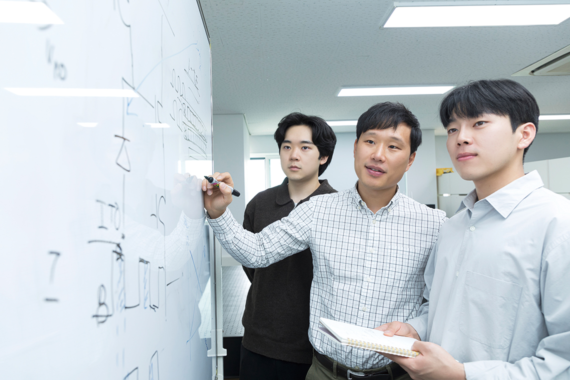
 Pixel Lab led by Professor Ji-won Lee. For a little over a year, many graduate students have been studying image sensor technology with Professor Lee.
IMEC’s only visiting professor from Korea
Professor Ji-won Lee is conducting research focusing on the design of next-generation image sensors based on his experience accumulated in the business world. He explains: “As the role of cameras among smartphone functions becomes more important, more cameras and image sensors are being introduced. In particular, with the development of image processing technology, more information can be obtained from images, expanding into a variety of applications. Accord-ingly, we are conducting various kinds of research aimed at developing image sensors to obtain more efficient information.”
Prof. Lee has obtained 12 overseas and seven domestic patents, and has published 12 SCI papers, including the one in Nature Electronics. It has been just over a year since he took his position at ERICA. He needed great courage to choose to open a university laboratory when he already had open and advanced research opportunities at IMEC. Having achieved more and at a faster pace than others at an early age, he had to plan the next step for himself, and instead of a more financially fruitful job, he chose to work at the university. Unlike at the global corporate research institute where he had worked, working at ERICA meant he had to build everything over again. The past year has been a series of challenges for Prof. Lee. Nevertheless, he said he feels rewarded as a professor in the atmosphere of the Department of Photonics and Nanoelectronics, where students are eager to learn. Fortunately, his laboratory is already growing little by little. He is now a visiting professor at IMEC and a professor at ERICA, conducting joint research based on partnerships and creating a path for international research exchanges for students.
“A person can’t even design a single chip all on their own. The more that various elements are integrated, the higher the level of completion. Therefore, research networking with IMEC is very important, both for our students and the IMEC research institute.”
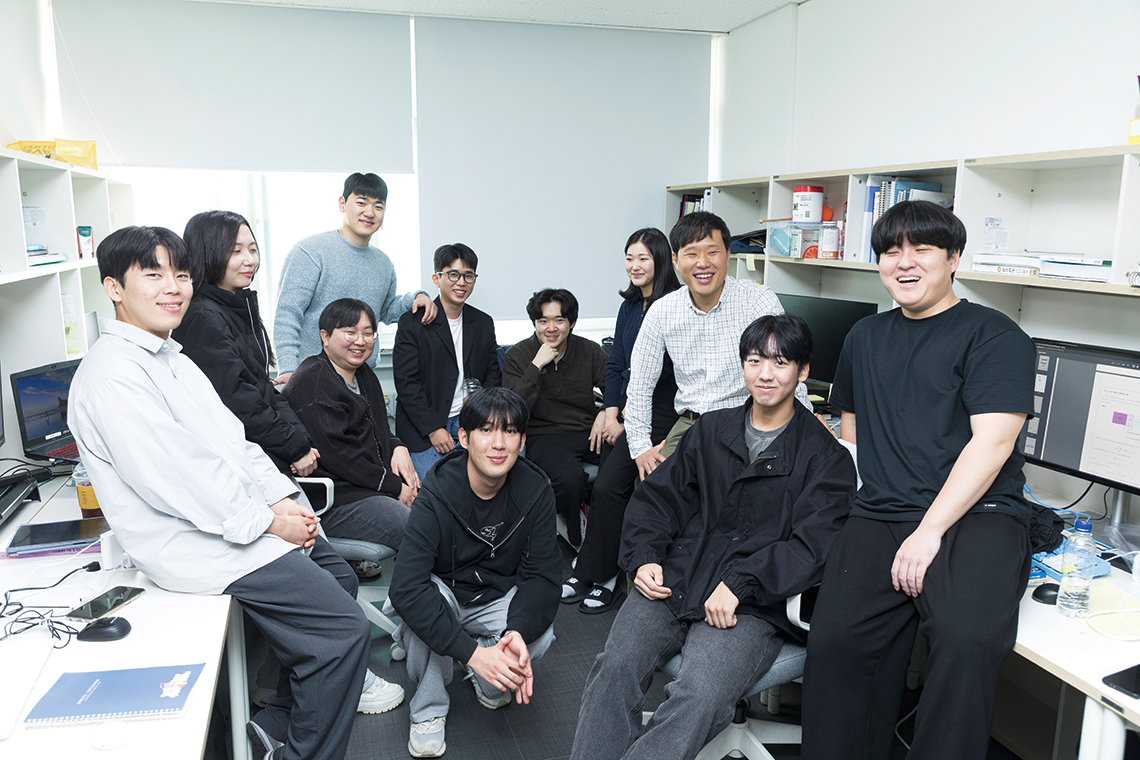
Prof. Lee stays in Belgium with his family every vacation to focus on his research. This winter, he plans to take his students from the Department of Photonics and Nanoelectronics to Belgium. Even though the laboratory is less than a year old, it has more than 10 graduate students. Prof. Lee feels much pressure to provide his students with a better research environment and more opportunities and experiences. However, he is also very ambitious.
“In the image sensor field, Korea has been in second place for a long time, behind Japan. I would therefore like to conduct diverse research and foster great talent so that Korea’s image sensor technology can be number one in the world.”